Reliability in HDI PCBs
High density interconnect (HDI) technology allows PCB designers to place components that are smaller and much closer together. This reduces component and trace lengths, enabling faster signal transmission and lowering power delivery impedance. However, as with all advanced technologies, there are some limitations and challenges that can be encountered when designing for HDI. Keeping these considerations in mind can help ensure reliability in your final product.
The HDI manufacturing process differs from the standard fabrication process in a few key ways. As a result, fabricator limitations can constrain your design choices. For example, if your design uses narrower traces and spaces, you will need to verify that these specifications are within the limits of the fabrication process you’re using. You will also need to know if the copper-to-edge clearance meets requirements for your manufacturer’s assembly and testing processes.
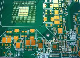
Another important consideration is the hdi pcb stack-up and via style that will be used to route signals through inner layers. You should work closely with your fabricator to obtain PCB stack-up information, including layer counts and dielectric thicknesses. You will want to ensure that the stack-up is designed for the manufacturing process and will meet your device’s performance and reliability needs.
How to Ensure Reliability in HDI PCBs
The most popular PCB stack-ups for HDI devices are blind and buried vias, which provide connections through multiple layers of the PCB. This approach requires multiple laminations and can be quite costly. However, if you are unable to use conventional through-holes for your device’s circuitry due to size or space constraints, this technique can allow you to meet your signal routing requirements with less cost.
Another common option for HDI devices is the use of laser microvias. These are created with laser drills that generate a laser at up to 20 microns in diameter, making it possible to create tiny but clean holes. However, it’s important to note that these holes can be more susceptible to drilling deviations and other defects than traditional through-hole vias.
Using a staggered arrangement of microvias is one way to minimize the risk of these concerns. Compared to stacked microvias, these arrangements can be more reliable and still allow you to route your signals.
While you can optimize your HDI PCB layout by understanding the limitations and challenges of the fabrication process, it’s important to work with your fabricator to ensure that your design meets their DFM (design for manufacturing) guidelines. By doing so, you can ensure that your device will be fabricated and assembled reliably. Start your free trial of Altium Designer today to get access to a complete set of tools for HDI PCB design, including an integrated design rules engine and Layer Stack Manager. Altium Designer makes it easy to collaborate with your fabricator and release files directly to them. Ensure your device is ready for manufacturing by checking your layer stack-up against the fabrication capabilities of your manufacturing partner, then calculate and account for impedance values with the built-in impedance calculator.