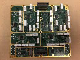
Commonly Used in RF PCB Fabrication
RF PCB fabrication is a complex process that requires careful attention to detail. The materials used must be able to provide stable electrical properties at high temperatures and also offer thermal robustness during assembly and soldering processes. RF PCBs must also be designed to prevent signal degradation through signal attenuation and interference from cross-talk, impedance mismatch, and other factors. This is necessary to ensure that the RF signals can travel across the board with minimal loss and distortion, ensuring the integrity of the final product.
While FR-4 is an acceptable material for low-frequency applications, it can have issues with higher frequencies. This is because FR-4 does not have a good dielectric constant (DF), which results in a large amount of energy being dissipated as heat during the signal transmission. This can cause problems with signal propagation and create other issues like electromagnetic interference that degrades the quality of the RF signals.
To avoid these issues, RF engineers use other specialized materials for their RF PCBs. PTFE and ceramic substrates are common choices for high-frequency PCB fabrication. These materials are more expensive than standard FR-4 laminates, but they can offer better performance and reliability in a wider range of operating conditions.
High-frequency laminates: Materials such as Rogers Corporation’s RO4000 series or Taconic’s TLY series are popular choices due to their low dielectric constant and loss tangent, providing excellent signal integrity at RF frequencies. Controlled impedance traces: RF signals demand precise impedance matching to minimize reflections and ensure maximum power transfer. Controlled impedance traces are achieved through careful design and manufacturing techniques, including specific trace widths and spacing.

What Materials Are Commonly Used in RF PCB Fabrication?
In addition to providing stable electrical properties at high temperatures, these specialized RF PCB materials must have a low CTE to ensure that the board will not warp or crack during fabrication and assembly. This is especially important for RF boards that require high amounts of drilling or will be deployed in thermally demanding environments, such as aircraft or automotive components.
The most commonly used rf pcb materials today are PTFE-based laminates from Rogers Corporation. This company produces a number of different RF laminates with various dielectric constants and frequency ranges, with some of them specifically optimized for the Ka band (car radar) and 5G bands.
When selecting a RF PCB design, it is important to consider the thickness of the copper layers. For mmWave applications, thinner copper layers can improve signal propagation and allow for smaller components to be placed closer together. It is also a good idea to make sure that the traces are as short as possible and to route them away from other critical components in order to minimize unwanted interference. Finally, it is essential to select a fabrication process that has experience working with these high-frequency materials. Failure to do so can result in defects such as solder joint failures and trace delamination. By following these guidelines, a designer can design an RF PCB that performs to the highest standards of reliability.


